Share
You are working as an electrical engineer in a factory that manufactures electrical components and circuits. You have been asked by your manager to prepare a printed circuit board of the following systems
ReportQuestion
Please briefly explain why you feel this question should be reported.

You are working as an electrical engineer in a factory that manufactures electrical components and circuits. You have been asked by your manager to prepare a printed circuit board of the following systems:
(a)
Design a basic op-amp based BJT or FET technology showing all stages. Do the basic analysis in terms of finding all dc voltages and currents in the circuit. Find the ac differential voltage gain, input and output impedance, current gain, common voltage gain, the common mode rejection ratio and slew rate.
(b)
Compare your results with the ones of 741 op-amps.
(c)
What is output stage classification (power amplifier) used in your circuit. Define your conduction angle and calculate efficiency.
(d)
Use your op-amp to design a first-order LP filter having a cut-off frequency of your choice.
(e)
Use your op-amp to design a basic non-inverting amplifier with a gain of 10V/V.
(f)
Use 741 op-amp to compare your results of section (b) and (c) with the results obtained if 741 op amp implemented.
(g)
Choose your op-amp and the right ADC to convert an industrial signal of changing frequency from 1kHz to 10kHz with amplitudes up to 10mV to digital 8-bit output. (Multisim).
Use Multisim to implement your design and the applications affiliated with your op-amp. Show all calculations and plots needed for the analysis and evaluation.
Answer ( 1 )
Please briefly explain why you feel this answer should be reported.
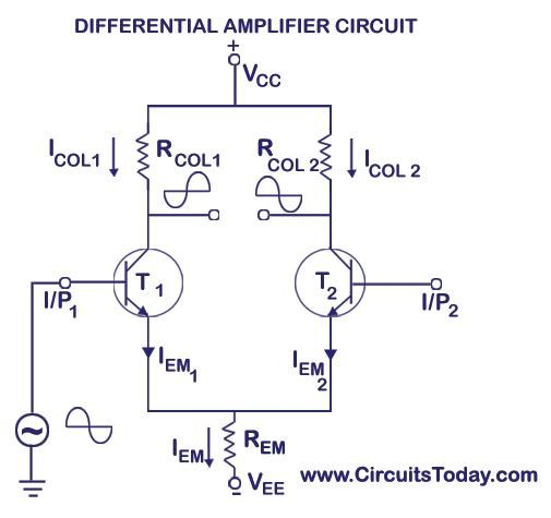
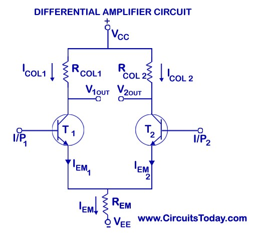
As shown in the circuit diagram above there are two inputs, I/P1 and I/P2 and two outputs V1OUT and V2OUT. I/P1 is applied to the base of the transistor TI and IP2 is applied to the base of the transistor T2. The emitters of both T1 and T2 are connected to a common emitter resistor so that the two output terminals V1OUT and V2OUT gets affected by the two input signals I/P1 and I/P2. VCC and VEE are the two supply voltages for the circuit. The circuit will also work fine using just a single voltage supply. You may have also noted that there is no ground terminal indicated in the circuit. Hence it must be automatically understood that the opposite points of both the positive and negative voltage supplies are understood to be connected to the ground.
Working of a Differential Amplifier
When a differential amplifier is driven at one of the inputs, the output appears at both the collector outputs. This is explained with a diagram below.